
555 Timer Tutorial:
www.powerintegarted.in

The 555 Timer, designed by Hans Camenzind in 1971, can be found in many electronic devices starting from toys and kitchen appliances to even a spacecraft. It is a highly stable integrated circuit that can produce accurate time delays and oscillations. The 555 Timer has three operating modes, bistable, monostable and astable mode.
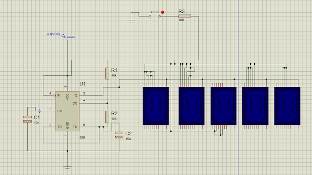
FIGURE 1 : 555 TIMER WITH SEGMENT DISPLAY.
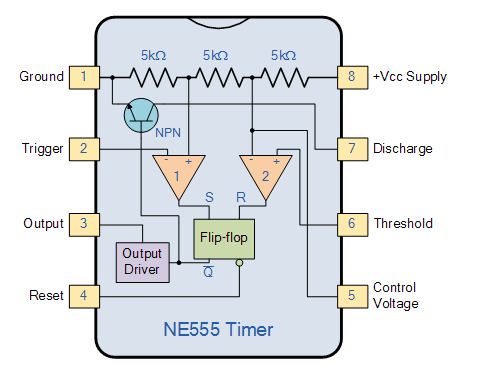
FIGURE 2 : 555 TIMER CIRCUIT.
www.powerintegrated.in
project centre in trichy.
PIN DETAILS:
- Pin 1. – Ground, The ground pin connects the 555 timer to the negative (0v) supply rail.
- • Pin 2. – Trigger, The negative input to comparator No 1. A negative pulse on this pin “sets” the internal Flip-flop when the voltage drops below 1/3Vcc causing the output to switch from a “LOW” to a “HIGH” state.
- • Pin 3. – Output, The output pin can drive any TTL circuit and is capable of sourcing or sinking up to 200mA of current at an output voltage equal to approximately Vcc – 1.5V so small speakers, LEDs or motors can be connected directly to the output.
- • Pin 4. – Reset, This pin is used to “reset” the internal Flip-flop controlling the state of the output, pin 3. This is an active-low input and is generally connected to a logic “1” level when not used to prevent any unwanted resetting of the output.
- • Pin 5. – Control Voltage, This pin controls the timing of the 555 by overriding the 2/3Vcc level of the voltage divider network. By applying a voltage to this pin the width of the output signal can be varied independently of the RC timing network. When not used it is connected to ground via a 10nF capacitor to eliminate any noise.
- • Pin 6. – Threshold, The positive input to comparator No 2. This pin is used to reset the Flip-flop when the voltage applied to it exceeds 2/3Vcc causing the output to switch from “HIGH” to “LOW” state. This pin connects directly to the RC timing circuit.
- • Pin 7. – Discharge, The discharge pin is connected directly to the Collector of an internal NPN transistor which is used to “discharge” the timing capacitor to ground when the output at pin 3 switches “LOW”.
- • Pin 8. – Supply +Vcc, This is the power supply pin and for general purpose TTL 555 timers is between 4.5V and 15V.
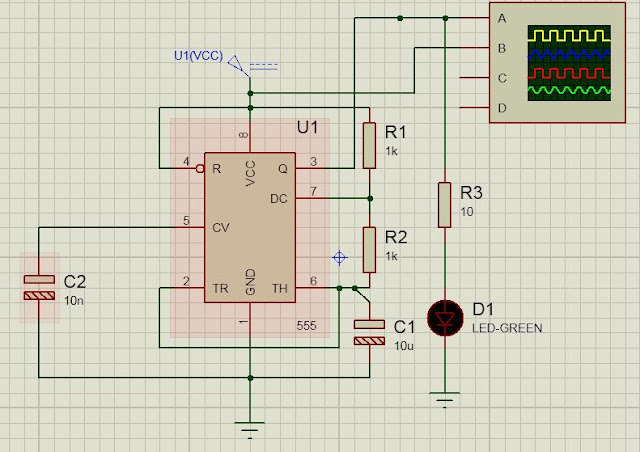
Finally Change the value of Capacitor and Resistor to see the change in Output Delay at PIN 3.
Thanks & Regards:
POWER INTEGRATED SOLUTIONS
No:10A/3,Radhakrishna Colony,Sasthri Road, Thennur, Trichy-17
.Mail to: powerintegratedsolutions@gmail.com
Visit to:www.powerintegrated.in
Call us: 0431-4340778 / 7639385448 / 9566377454.